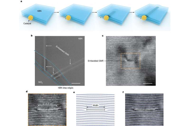
Directly grown embedded graphene nanoribbons. Credit: Nature (2024). DOI: 10.1038/s41586-024-07243-0
An international collaborative study that features researchers from Tel Aviv University (TAU), presented a new method for growing ultra-long and ultra-narrow strips of graphene (a derivative of graphite), which exhibit semiconducting properties that can be harnessed by the nanoelectronics industry. The researchers believe that the development may have many potential technological applications, including advanced switching devices, spintronic devices, and in the future, even quantum computing architectures.
The study was conducted under the leadership of an international research team that included Prof. Michael Urbakh and Prof. Oded Hod from TAU’s School of Chemistry, as well as scientists from China, South Korea, and Japan. The study was published in the journal Nature.
Prof. Urbakh and Prof. Hod explain that graphene is actually a single layer of graphite made of carbon atoms and built similar to the shape of a beehive. Graphene is very suitable for technological uses.
Apart from its extraordinary mechanical strength, additional properties have been discovered in recent years regarding certain structures made of a small number of twisted (laterally rotated with respect to each other) graphene layers. These properties include superconductivity, spontaneous electric polarization, controlled heat conduction, and structural superlubricity—a state in which materials demonstrate negligible friction and wear.
One of the limitations for the use of graphene in the electronics industry is that it is a semi-metal, namely that charge carriers can move freely in it, but their density is very low. Hence, graphene cannot be used either as a conducting metal or as a semiconductor used by the electronic chip industry.
However, if long and thin strips of graphene (termed graphene nanoribbons) are cut out of a wide graphene sheet, the quantum charge carriers become confined within the narrow dimension, which makes them semi-conducting and enables their use in quantum switching devices. As of today, there are a number of barriers to using graphene nanoribbons in devices, among them is the challenge of reproducibly growing narrow and long sheets that are isolated from the environment.
2024-05-20 11:00:02
Original from phys.org


